Leadership in enabling and industrial technologies - ICT - PETMEM
H2020 LEIT ICT
PETMEM (Piezoelectronic Transduction Memory Device) is a European Commission funded project under the H2020 ICT Programme. PETMEM is a European partnership amongst Universities, Research Institutions, SMEs and a large company that will focus on the development of new materials and characterization tools to enable the fabrication of an entirely new low-voltage, memory element.

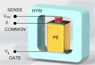
PETMEM is a European partnership amongst Universities, Research Institutions, SMEs and a large company that will focus on the development of new materials and characterization tools to enable the fabrication of an entirely new low-voltage memory element. This element makes use of internal transduction in which a voltage state external to the device is converted to an internal acoustic signal that drives an insulator-metal transition. Modelling based on the properties of known materials at device dimensions on the 15nm scale predicts that this mechanism enables device operation at voltages an order of magnitude lower than CMOS technology (power is reduced two orders) while achieving 10GHz operating speed. Additional, possibly earlier development applications include ultralow power RF switches for telecommunications devices and low voltage several GHz logic devices especially for portable equipment. The consortium that will develop PETMEM technologies comprises 11 partners: Bio Nano Consulting (London UK), IBM Research (Zurich, Switzerland), Max Planck Institute (Dresden and Halle, Germany), Solmates (Enschede, The Netherlands), SINTEF (Oslo, Norway), National Physical Laboratory (Teddington UK), University of Gent (Gent, Belgium), EMPA (Switzerland), Aixacct (Aachen Germany), Electrosciences (Surrey, UK) and DCA (Turku, Finland).
Objectives
These are the objectives of PETMEM:
- Technological objective: demonstrate the PETMEM proof of concept by fabricating working devices
- Scientific objective: establish a fundamental understanding of the new materials and novel nanoscale structure
- Innovation objective: increase EU market share in the production of piezoelectric transduction devices
Role of Ghent University
The role of Ghent University is the deposition, optical and structural characterization, and optimization of piezoresistive, chalcogenide layers based on samarium sulfide (SmS). The experimental work mainly includes scaling the deposition process to larger wafer size and alloying the SmS by other (lanthanide) elements to modify the switching behavior of the SmS between the semiconducting and metallic state.
Contact
Prof. Philippe Smet
Department of Solid State Sciences
Phone number: +32 9 264 43 53
E-mail: philippe.smet@ugent.be