Test & Research Infrastructure

Overview of the available test and research infrastructure

Cleanroom

The equipment for fabrication and characterization at the nano- and micrometer scale is located in the Ghent University cleanroom building at campus Ardoyen.

The cleanroom is an environment where we limit the presence of sub-micron particles and control other factors such as temperature and humidity. This is necessary to achieve sound manufacturing processes that ensure reproducible results.

UGent cleanroom infrastructure located at the campus Tech Lane Ghent Science Park

Equipment for lithography (pattern definition)

EVG 620 double-sided mask aligner

The mask aligner is used to transfer a pattern to a photosensitive material by selective exposure (through a mask) to a UV radiation source. The equipment supports several modes (proximity, soft / hard / vacuum contact) and can also do bottom side alignment. It can also be used in nano-imprint mode, where the pattern is transferred by imprinting.

EVG 620 double-sided mask aligner

Heidelberg DWL66 Laser Direct Imaging

The Heidelberg DWL66 LDI system uses laser direct imaging (LDI) to expose photosensitive materials with resolution down to 1 μm. Laser: 250mW @ 355nm.

Heidelberg DWL66 Laser Direct Imaging

Voyager EBEAM

50kEV Electron beam lithography for defining patterns with resolution down to 10 nm. Pattern generator 20bits, 500μm writing field. For samples and wafers up to 200mm. Traxx option for continuous writing of structures (fixed beam, moving stage).

 Voyager EBEAM

MA6 mask aligner (I)

Optical Lithography system. Definition of patterns in photosensitive layers with resolution down to 800nm. Option for backside alignment. For samples and wafers up to 150mm.

 SUSS MicroTec MA6/BA6 aligner

MA6 mask aligner (II)

Optical Lithography system. Definition of patterns in photosensitive layers with resolution down to 600nm. Option for deep UV lithography (248nm). For samples and wafers up to 150mm.

 SUSS MicroTec MA6 aligner

Equipment for layer deposition

Advanced Vacuum Vision 310 PECVD

Plasma deposition system for accurate deposition of SiO2, Si3N4 and a-Si layers using a plasma enhanced chemical vapor deposition process.

Advanced Vacuum Vision 310 PECVD

Spinner

Diverse spinner for spincoating polymer layers including photosensitive resist layers. For samples and wafers up to 200mm.

Polos spin coater

Electron Beam Evaporator

Evaporation of insulating and conducting layers on diverse samples through heating with electron beam. Can be used for accurate deposition of thin metal layers or coatings.

Electron Beam Evaporator

Trovato thermal evaporation system

Thermal evaporation system designed for deposition of organic layers. Includes Marathon CP-8 Cryopump and Innovative Technologies glove box (N2 atmosphere).

Trovato evaporation system

Equipment for material structuring

3D Micromac microSTRUCT vario ps/fs Laser setup

Pico- and femtosecond laser setup ideally suited for laser structuring, cutting, drilling and welding applications on a variety of substrates, e.g. metals, semiconductors, alloys, transparent and biological material, ceramics and thin film compound systems. The setup is equipped with following lasers: femtosecond pulse laser at 1030.5nm; picosecond pulse laser at 1064nm, 532nm and 355nm

3D Micromac miscrostruct vario ps/fs Laser setup

Optec multilaser setup

The custom build multilaser setup is equipped with three different lasers: an excimer laser at 248nm, a CO2 laser at 9 to 11um and a ND-Yag laser at 354.7nm.

Optec multilaser setup

DISCO DAD322 Dicing machine

The Disco DAD322 is a fully automated dicing saw to cut materials such as silicon wafers and glass substrates.

DISCO DAD322 Dicing machine

Logitech PM5 Precision Lapping and Polishing System

The Logitech PM5 Lapping and Polishing Machine is a workstation that is used for the back-thinning of individual dies. The individual chip thinning technology was optimized for Silicon chips as well as for GaAs /InP Opto-Electronic components.

Logitech PM5 Precision Lapping and Polishing System

Vacuum laminating press (Lauffer RLKV 25)

Automated vacuum lamination press with controlled temperature and pressure profiles for 330 mm by 280 mm substrates.

Lauffer RLKV 25 Vacuum laminating press

Vacuum forming machine (Formech 300XQ)

Vacuum forming of thermoplastic materials using an infrared heater.

Formech 300XQ vacuum forming machine

Equipment for etching

Large area processing line for flex PCB

Degrease/μ-etch, development, etch and strip line for 12” by 9” flexible PCBs combined with a Bungard Large area UV exposure machine.

Large area processing line for flex PCB

Advanced Vacuum Vision 310 RIE

RIE plasma etch system for etching of diverse materials including glasses, SiO2, Si3N4, Silicon, Germanium, polymers ...

Advanced Vacuum Vision 320 RIE

Oxford ICP System 100 (I)

ICP plasma etch system for etching of diverse materials including glasses, SiO2, Si3N4, Silicon, Germanium, polymers ...

Oxford plasmalab system 100 (I)

Oxford ICP System 100 (II)

ICP plasma etch system for etching of diverse materials including III-V semiconductors.

Oxford plasmalab system 100 (II)

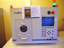
PVA TEPLA Plasma etch

Oxygen plasma tool for cleaning of samples. Can also be used for activation/surface modification of polymers and glasses used in microfluidic circuits.

PVA Tepla plasma etch

Critical point dryer

Allows to release MEMS like structures (micromechanical structures)

Leica Microsystems critical point dryer

Wet benches and exhaust benches

More than 10 wet benches for safer working with chemicals, including acids, bases and solvents. Wet benches allow for clean working (class 100)

Wet benches and exhaust benches

Equipment for inspection

FEI Nova 600 Nanolab Dual-Beam FIB-SEM

SEM (Scanning Electron Microscope) can be used for inspection of samples with resolution down to nanometer scale. The FIB (Focused Ion Beam) column can be used for making cross-sections in virtually any material and gives the option to look "into" the material. FIB also allows to directly pattern materials with nanometer resolution. Options include electron backscatter diffraction (EBSD, for evaluation of microstructure of material), several etch gas injectors, Auto-slice&View and nanomanipulators for TEM-slice preparation.

More information

 FEI Nova NanoLab Dual beam FIB-SEM

JEOL JSM-6500 SEM incl. Energy Dispersive Spectroscopy (EDS)

Imaging using a scanning electron beam and several detector heads : secondary electrons, back-scattered electrons, cathodo-luminescent photons. Elemental analysis using electron dispersive spectroscopy is also possible.

 JEOL JSM-6500 SEM + EDS

JSM-7000F TFEG-SEM with JED-2300F EDS

In order to obtain higher resolution and smaller spot sizes for analysis, a field emission gun scanning electron microscope (FEG-SEM) is indispensable.

 JEOL JSM-7000F TGEG-SEM with JED-2300F EDS

WYKO NT3300 non-contact optical profiler

A white light interferometer is capable of mapping a several millimeter wide area in a single measurement, with sub-nanometer resolution, providing instantaneous information about surface roughness, shape and waviness.

 WYKO NT3300 non-contact optical profiler

Nikon Eclipse LV100 Inspection Microscope

Microscopic inspection and image capturing / measuring of samples. Equipped with 15 X oculars for a standard magnification range of 75 X to 1500X, Nomarski prisms, and episcopic and diascopic filters.

 Nikon Eclipse LV100 Inspection Microscope

JEOL IB-09010CP Ion beam cross section polisher

Polishing cross-section surfaces by using an ion beam. This instrument uses accelerated Argon ions (at 2 to 6 kV) to precisely remove material from the sectioned sample.

 JEOL IB-09010CP Ion beam cross section polisher

Olympus DSX 500 microscope

Automated microscope with options for measurement and 3D-visualisation, darkfield microscopy ...

 Olympus DSX 500 microscope

Veeco Dektak

Profilometer, for measuring step heights on samples with range varying from few nanometer to several 100 micrometer.

 VeeCo Dektak 150 surface profiler

Equipment for assembly

Tresky die and flip-chip bonder

Die and flip-chip bonder for the assembly of bare-die components with and accuracy of ± 5 μm.

 Tresky die and flip-chip bonder

K&S Manual Wedge Bonder model 4523

Manual wedge bonding of:

  • aluminium wire: 18um and 32um, 30/45deg and deep acces wedges.
  • gold wire: 38um (deep acces) and 76.2x25.4 ribbon (deep acces).

This model offers the versatility to bond simple discrete devices, chip on board, up to complex hybrid, microwave devices. A bonding head with a deep access option and tail adjust system supports deep cavity microwave applications where tight control over the tail length is essential. With the small 18um wire capability the creation of short wires with low loops to support RF devices is possible. A manual Z mode allows operator control over looping and wire length, providing excellent resuslts for tight spaces or unusual loop requirements.

K&S Manual Wedge Bonder - model 4523

Finetech Pick and Place

Accurate (±1 micrometer) placement of chips and other 3D-structures.

 Finetech Pick and Place

X-Celeprint μTP-100 Transfer Printer

Accurate and automated (±1 micrometer) placement of thin layers of materials.

 X-Celeprint μTP-100 transfer printer

SUSS MicroTec Wafer Bonder

Wafer bonder for samples and substrates up to 150mm. Compatible with thermal bonding and pressure bonding. Aligned bonding fixtures available. Allows creating heterogeneous substrates containing diverse materials not otherwise integrable.

 SUSS MicroTec Wafer Bonder

EVG 501 Wafer Bonder

Wafer bonding tool for substrates up to 200 mm wafers.

 EVG 501 Wafer bonder

GDP global dispenser

Automated needle dispenser for controlled deposition of adhesives or solder paste.

 GDP global dispenser

EKRA E4-STS Screen printer

Fully automatic screen printer for accurate deposition of adhesives or solder paste using either screens or stencils.

 EKRA E4-STS Screen printer

IBL SLC 300 Vapour phase reflow oven

Reflow oven for solder pastes with a programmable temperature profile using the vapour phase of an inert liquid for the transfer of heat.

 IBL SLC 300 Vapour phase reflow oven

Optomec 300-UP Aerosol Jet Printer

The aerosol-jet system is used to print metallic conductive inks (silver, gold, copper, etc.) based on creating an aerosol of a functional liquid ink and focusing the aerosol stream on the substrate by a nitrogen gas flow.

 Optomec 300-UP Aerosol Jet Printer

Liquid crystal device assembly

Several devices for assembly of liquid crystal devices including spin coater, dip coater, Asymtek Dispensemate, Oxford Instruments rubbing machine, UV OmniCure UV illumination, several ovens (including high temperature annealing oven), temperature controlled vacuum filling equipment, inspection microscope.

 Liquid crystal device assembly

Equipment for testing

CTS CS-40/200 climate chamber

Climate chamber for Thermal cycling (-40°C/+150 °C, 6°/min) and Temperature-Humidity (10 - 95 °C,10 – 98 % RH).

 CTS CS-40/200 climate chamber

Votsch VTS 7040-15/S climate chamber

Climate chamber for Temperature cycling (-70 °C to 180 °C, 16 °/min) with in-situ resistance measurement.

 Votsch VTS 7040-15/S climate chamber